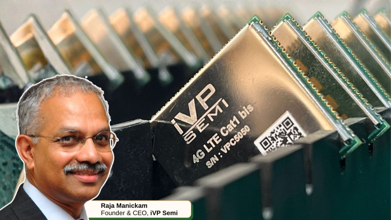
Building an Indian Chip Brand | Raja Manickam

Raja Manickam is a semiconductor industry veteran and the Founder & CEO of iVP Semi, a fabless semiconductor firm based out of Chennai. We discuss India’s current semiconductor landscape, the role semiconductors play in EVs and iVP Semi’s work in the domain.
Where does India stand today in the global semiconductor value chain when we discuss building a complete ecosystem—including fabrication plants (fabs), ATMP (Assembly, Testing, Marking, and Packaging) units, and the supply chain?
The semiconductor ecosystem has multiple parts: design, manufacturing, embedded systems and the software that goes with the chip. On the manufacturing side, we have a negligible footprint today. While there is a strong aspiration to play a larger role, the government is currently the primary driver in enabling this shift. However, it is important to realise that India already possesses almost all the other essential ingredients.
Even though they are not domestic firms, global leaders in EDA (Electronic Design Automation) tools, such as Texas Instruments, Intel, AMD, and NVIDIA, have a massive presence here. A significant portion of critical engineering, design, and silicon bring-up happens in India, largely through Global Capability Centres (GCCs). While we may feel excluded from the physical supply chain, our engineering piece is very strong. Over the next decade, these multinationals can provide the foundation for Indian companies to emerge. While the government is seeding manufacturing, the next step requires greater private-sector participation.
Given the current landscape, which specific parts of the semiconductor value chain can we realistically work on? And which areas can Indian companies start with?
The global market is shifting toward three distinct supply chains: the American, the Chinese, and the rest of the world. I believe India can take the lead in this third supply chain, especially by leveraging strategic partnerships like the recent Europe-India Free Trade Agreement. Hopefully, Japan joins in as well, and we’ll have a huge opportunity. In terms of specific segments, we certainly have an upper hand in design, due to our immense engineering talent and strong global diaspora. Over the next decade, I believe Indian firms can dominate this space and transition into fabless product companies like NVIDIA and others.
While physical manufacturing will take more time to build—likely over the next 10 years—we can immediately focus on equipment manufacturing. Currently, nearly 100% of semiconductor equipment is imported. We have a massive opportunity to manufacture this equipment locally through joint ventures or by becoming suppliers to established global players. Players like Applied Materials and LAM Research are also pushing for more sourcing out of India.
Materials and processes will take longer to develop (currently dominated by Japanese players), design and equipment making are our best doors into the industry.
Under the India Semiconductor Mission, there have been major announcements, such as the Tata-PSMC joint venture aiming to roll out chips by late 2026. In your opinion, how realistic are these estimates?
2026 is definitely not possible, though it is often helpful to set a lofty goal to gather momentum and align the industry. This is the first time India is attempting this at such a massive scale, and it is being led by players like Tata, CG Power, and Kaynes, who have not been in this space before. A primary reason for their entry into this space is the significant government subsidy.
Realistically, we are looking at a 3 to 4-year timeline. I do not expect to see wafers and volume production until 2028, though we might see initial testing activity in the second half of 2027. It is important to distinguish between “fab” and “packaging” (ATMP). Packaging uses mature technology and can be set up in 3 to 6 months once the building is ready. Fabrication, however, will take much longer. The most important thing is that we have finally made a start.
Could you explain the ‘fabless’ model? Why is this approach advantageous for an Indian company like iVP Semiconductor?
I started my career in the early 80s. Back then, companies like Texas Instruments (TI) were fully vertical—if you wanted to make a chip, you needed a fab, the equipment, and also packaging and testing. Everything was done in-house. Over time, the industry became specialised. Today, you have different specialists for fab equipment like lithography and deposition, and separate companies focused only on packaging tools like wire bonders and molds.
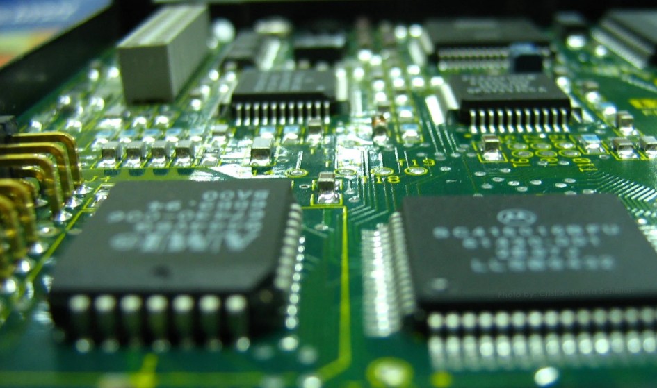
So, in the mid-80s to early 90s, the fabless model emerged. Designers from companies like Intel and AMD realised they could focus solely on design and outsource fabrication, without owning any manufacturing assets. That’s what fabless companies do, and it’s also the most profitable part of the value chain because you don’t invest in heavy assets. iVP Semi follows the same model.
And Intel is a classic example of the old model—owning fabs meant a lot of investment went into manufacturing instead of products, making it harder to compete with fabless companies like AMD and NVIDIA. That’s why fabless is the future, and India will likely follow the same model too.
In the fabless model, how much (beyond fabrication) is typically outsourced?
Everything related to manufacturing—including packaging—is typically outsourced. In fact, even within the design phase, many companies choose to outsource specific elements or even full designs to specialised service providers. In my previous company, Tessolve, we focused on providing exactly these kinds of design and post-wafer services to global players.
The true role of the fabless company is to be the “integrator”—the entity that puts all these specialised pieces together and manages the final product.
This is indeed the model most Indian semiconductor companies are following today: focusing on the core design and orchestration while outsourcing the rest of the value chain.
How do Tessolve and iVP differ in terms of their offerings?
Tessolve is a service company, similar to a “TCS-type” organisation, but focused on the semiconductor industry. Its core strength lies in post-wafer fab services, specifically test and test development. My first job was as a test engineer at TI, so that’s my forte. While Tessolve supports global giants like Intel, TI, and Qualcomm with design and hardware work, it does not have its own products or branding. In contrast, iVP is a product company. My goal is to establish iVP as a globally recognised Indian chip brand—comparable to TI, NXP, STMicro or NVIDIA. Currently, India lacks a domestic brand even for simple components like MOSFETs or diodes. I want iVP to fill that gap and become a true Indian chip company.
We are already selling products in the market under the iVP brand. As a fabless company, we handle some of the design in-house and outsource the rest.
Because there is currently no wafer fabrication plant in India, our chips are fabricated in Taiwan and Japan. At present, they are packaged in Malaysia and the Philippines, though we intend to bring packaging to India as soon as that domestic capability exists. We perform testing in-house before selling the final chips to our customers under the iVP brand.
Who are your primary customers, and how are you engaging with the EV sector?
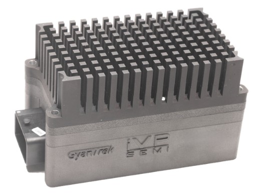
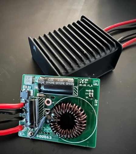
iVP is heavily focused on the power segment, providing components like MOSFETs, diodes, LDOs, gate drivers, and various subsystems. Our primary targets are the EV and renewable energy sectors, serving Indian OEMs and their supply chains.
For example, we’re talking to Mahindra, suppliers to Mahindra and Tata as well as TVS Lucas—two-wheeler electrification suppliers. We also have business in renewable energy, supplying inverters, transformers, and even white goods that require power components.
Could you explain the specific role semiconductors play in an EV? Using an e-2W as an example, which parts are most dependent on semiconductor technology?
In EVs, and specifically two-wheelers, the traditional engine is replaced by an electrical motor, making nearly every system dependent on electronics. A primary area is the Battery Management System (BMS), which uses semiconductors to regulate the battery—controlling how it charges, discharges, and switches on or off. Beyond the battery, semiconductors are essential for:
- Power Switching: Basic transistors handle everything from switching lights to managing high-power electrical flow.
- Motor Control Unit: This acts as the electrical equivalent of an engine control unit, managing the vehicle’s propulsion.
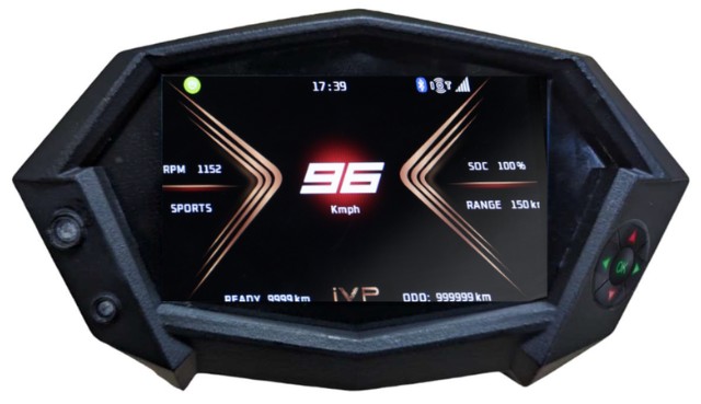
- User Interface: Modern EVs feature sophisticated digital clusters and displays that require significant processing power to monitor electrical measurements in real-time.
- Safety and Intelligence: Sensors placed throughout the vehicle monitor equipment health and improve the driving experience. For instance, a vehicle can detect a slippery slope via semiconductor-based sensors, which then feed data to a processor to automatically apply the necessary braking or motor control.
When you say you’re talking to companies making motors and controllers—what is the physical product that you will supply to them?
We supply what we call “discretes”—which include MOSFETs, gate drivers, LDOs, and DC-DC converters. In addition to these individual components, we provide “subsystems” such as half-bridge and full-bridge modules, along with thermal management-related solutions.
These are designed as “plug-and-play” offerings, allowing our customers to focus on the mechanical and driving aspects of the vehicle while we handle the internal electronics. In electronics, the fundamental thing is choosing the right chips. Performance improvements, cost improvements, and power conservation—all of that happens at the chip level. If you can optimise those, you end up with a superior product.
Is there a software component integrated into the products you supply, or is the software development handled entirely at the OEM level?
Software in this context consists of several different layers. At the chip level, we manage the operating system layer and the communication protocols between chips, commonly known as drivers. We also handle the integration of the controller with our power modules.
In this partnership, we provide the “guts” of the internal software that makes the hardware function. This allows the OEM or end customer to focus on the top-level aplication, which includes the user experience, interface, and the overall “look and feel” of the vehicle.
Are your products standard offerings or customized for specific requirements?
Our current phase focuses on standard products to facilitate quick market entry. It’s basically a replacement model—big companies already supply certain MOSFETs or LDOs, and we have the exact same chip, allowing customers to easily swap their current parts with our chips. This helps us gain immediate access to the market and establish ourselves as a trusted vendor.
Once integrated into their supply chain, we plan to collaborate on their future roadmaps and provide more bespoke support. Many Indian customers are eager for this level of engagement as they are often not treated as Tier 1 priorities by major global chipmakers; for us, they are a primary focus.
Could you tell us about your team and operational setup?
We currently have offices in both Chennai and Bangalore. In Bangalore, we are located in Electronic City—actually returning to the same building where I originally founded Tessolve. We have a team of ~65 people, with more than 50 dedicated to development, including chip and subsystem engineering. Beyond India, we have a team of 4 employees in Taiwan and are in the process of establishing an office in Singapore. This Singapore base will be essential for managing our supply chain, as our wafers and related components are currently sourced from outside the country.
Are iVP’s chips already being used in vehicles on the road, or are you in the customer qualification phase?
Most of our products are currently in the customer qualification phase. However, over the past few months, we have seen some products enter the market, though not yet in high volume. Customers are conducting field trials and have placed initial orders, particularly for display-related components. Looking ahead, my goal is for iVP to secure a sizable market share of 50% or more within the next five years across both the renewable energy and electric 2W sectors.
What policy interventions do you recommend to help Indian companies create globally competitive products?
Historically, the world’s leading semiconductor product companies were founded by passionate, technology-driven individuals rather than established corporations. My recommendations are:
- Support for “Moonshot” Founders: This is a deep-tech industry that requires high risk-taking. From a policy standpoint, the government should take the lead in funding passionate founders, as the private sector in India is often too risk-averse for R&D. Even if some fail, the learning generated is what builds a world-class ecosystem.
- Mandating Local Equipment Manufacturing: Currently, a vast amount of government funding is spent on importing manufacturing equipment. We need a policy that mandates a certain percentage—30–40%—of that equipment be manufactured in India within the next five years.
- Addressing Tax Disparities: Companies receiving grants under the India Semiconductor Mission enjoy tax exemptions on equipment, while independent startups investing their own capital are burdened by high import taxes, sometimes as high as 30%. Levelling the tax playing field is essential to encourage more private investment in the sector.
This interview was also published in EVreporter Feb 2026 magazine.
Also read: Role of Power Chips in EVs in 2026
Subscribe & Stay Informed
Subscribe today for free and stay on top of latest developments in EV domain.